Recently, Professor Liu Zhiqi and Professor Jiang Chengbao from the School of Materials Science and Engineering at Beihang University have made progress in the research of magnetic storage materials, and the related results were published as a full-text Article in Nature, entitled “Room-temperature magnetoresistance in an all-antiferromagnetic tunnel junction”. Qin Peixin, a PhD candidate in the School of Materials Science and Engineering, is the first author, and the School of Materials Science and Engineering of Beihang University is the first affiliation. Professor Liu Zhiqi and Professor Jiang Chengbao are corresponding authors of the first affiliation. Associate Professor Zhang Jia from the School of Physics of Huazhong University of Science and Technology and Researcher Zeng Zhongming from Suzhou Institute of Nano-Tech and Nano-Bionics, Chinese Academy of Sciences are the co-author and the corresponding author, respectively.
Magnetic materials are of great importance as one of the core materials in advanced technology fields such as aerospace, information and communication, and smart cities. As early as the Warring States period, the ancient Chinese people invented the natural magnetic spoon “Si Nan” to identify the direction. During the second Industrial Revolution period, symbolized by the advent of electricity, magnetic functional materials were essential for the conversion of electrical energy in generators and motors. In the information age of the third Industrial Revolution, magnetic functional materials are the core materials for hard disk drives as large-scale data storage devices.
Compared with traditional semiconductor materials and devices, magnetic storage materials and devices based on spintronics have the advantage of irradiation resistance under special environment in air and space, and play a key role for the development of aerospace information technology. Antiferromagnetic materials are a new class of magnetic storage materials, as data storage media, adjacent data bits can be closely aligned to enhance storage density, and the spin dynamics of antiferromagnetic materials are faster, promising next-generation highly integrated and ultrafast memory devices.
Most antiferromagnetic spintronic devices based on the relativistic anisotropic magnetoresistance mechanism exhibit very small electrical signal outputs at room temperature of around 0.1%. This has, to a large extent, prevented the utilization of antiferromagnets for practical information device applications. To address this challenge, the research team has made a breakthrough in the key technology of atomically fabricating flat antiferromagnetic thin films, which induces lattice tetragonal changes in non-collinear antiferromagnetic single-crystal films through interfacial stresses, resulting in uniaxial magnetic anisotropy and a significant anomalous Hall effect. Based on this anomalous Hall effect, the exchange bias effect at the all-antiferromagnetic heterogeneous interface (collinear antiferromagnetic/non-collinear antiferromagnetic) was experimentally discovered, leading to the design and preparation of a new all-antiferromagnetic tunnel junction (AATJ) device for multilayer films (See Fig. 1), which is the first time in the world to achieve an all-antiferromagnetic tunneling magnetoresistance with large nonvolatile room-temperature magnetoresistance values that reach a maximum of about 100% (See Fig. 2).
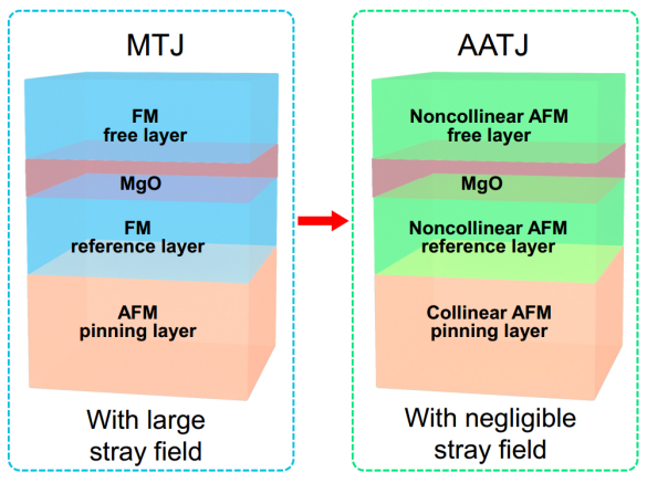
Fig. 1: Schematic of an AATJ.
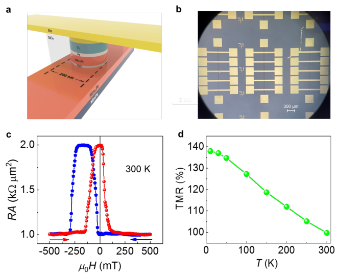
Fig. 2: AATJ microstructure and functional properties. a. Schematic of a nanoscale (200 nm) tunnel junction device. b. Optical image of patterned tunnel junction arrays. c. Room-temperature TMR as a function of the out-of-plane magnetic field for a typical nanoscale AATJ device. d. Temperature-dependent TMR.
Compared to the conventional in-plane electron transport antiferromagnetic memory device, this research has enabled the development of AATJ with perpendicular electron transport and an increase in room temperature electrical signal output by nearly three orders of magnitude, thus enabling the development of an ultra-fast response ultra-high density antiferromagnetic RAM-ARAM (See Fig. 3).

Fig. 3: Schematic view of a multi-layer stacked, densely arranged ARAM.
Link to the article:
https://www.nature.com/articles/s41586-022-05461-y
Reviewed by Li Jianwei
Edited by Jia Aiping
Translated by Li Yifan