A review article entitled "Solution-processed nano-LEDs for next-generation optoelectronic technologies,"co-authored by Professor Luo Deying and Associate Professor Yang Wenqiang from the International Institute for Interdisciplinary and Frontiers, Beihang University, together with collaborators, has been published online in Nature Photonics.
Focusing on two classes of solution-processable light-emitting materials—colloidal quantum dots and halide perovskites—the paper systematically reviews advances in nano-light-emitting diodes (nano-LEDs) covering materials chemistry, device engineering and nanofabrication. It analyses the trade-offs among luminous efficiency, operational stability and scalable manufacturing as pixels are miniaturized, and prospects applications in biophotonics, on-chip optical interconnects and super-resolution microscopy.
Associate Professor Yang Wenqiang (International Institute for Interdisciplinary and Frontiers, Beihang University), Researcher Ren Aobo (University of Electronic Science and Technology of China), Associate Researcher Yang Xiaoyu (Peking University), and Wang Hao (School of Instrumentation and Optoelectronic Engineering, Beihang University) are co-first authors. Professor Tae-Woo Lee (Seoul National University) and Professor Luo Deying (International Institute for Interdisciplinary and Frontiers, Beihang University) are corresponding authors. The International Institute for Interdisciplinary and Frontiers, Beihang University, is the first affiliation.
Driven by developments in augmented and virtual reality, optical sensing and on-chip optical interconnects, light sources demand smaller footprints, higher integration density and precise spatiotemporal modulation. The review addresses electrically driven nano-LEDs with sub-micrometre light-emitting pixels. Such devices hold promise for higher pixel density arrays, lower power consumption and faster modulation speeds, supporting emerging applications including on-chip optoelectronic integration and optogenetic neural interfaces.
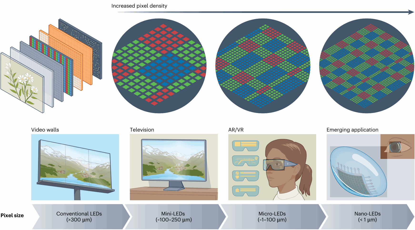
Pixel densities continue to increase with the development of LED technology for different application scenarios
The paper highlights that sidewall defects and interfacial effects become increasingly dominant as pixels shrink. Defect-induced non-radiative recombination, unbalanced charge injection, leakage current and localized heat accumulation are tightly coupled, limiting luminous efficiency and stability. In dense arrays, leakage currents and lateral light propagation can further introduce electrical and optical crosstalk between adjacent pixels. Coordinated optimization of surface chemistry, carrier transport, patterning protocols and device architecture is therefore required to mitigate performance degradation upon miniaturization.
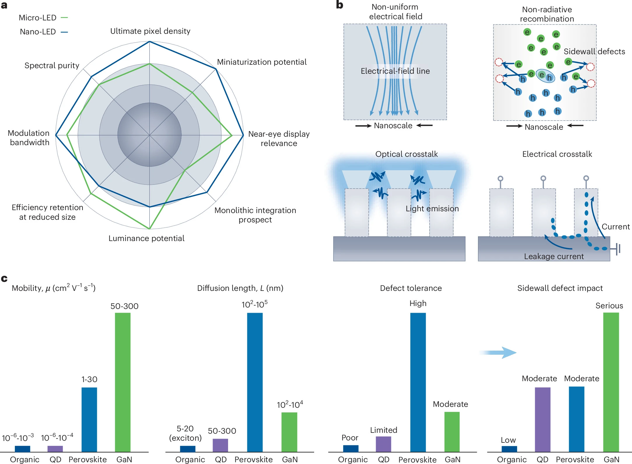
Impact of a sidewall defect in nano-LEDs
Colloidal quantum dots feature tunable emission colour, narrow linewidths and solution processability, making them attractive candidates for high-colour-purity nano-LEDs. The review summarizes strategies including surface ligand engineering, core-shell design and ordered assembly to suppress defect losses, improve charge transport and stabilize emissive layers. It also compares patterning techniques such as photolithography, electrophoretic deposition, transfer printing and nanoimprint lithography. Transfer printing minimizes fabrication damage and enables heterogeneous integration; nanoimprint lithography combined with capillary self-assembly offers a viable route for high-fidelity, parallel fabrication of nanopixel arrays.
Halide perovskites combine advantages such as high defect tolerance, tunable emission wavelength and low-temperature processing, and are likewise important candidate materials for achieving high-efficiency nano-LEDs. Research has already shrunk perovskite light-emitting pixels to approximately 90 nanometres and mitigated miniaturization-induced performance losses through designs such as localized contacts. However, such materials are sensitive to polar solvents, moisture and chemical processing, and processing-induced interfacial degradation and ion migration may still affect device efficiency and lifetime. Therefore, developing mild patterning processes and reliable encapsulation technologies is an important direction for improving device stability.
The paper emphasizes that no single material platform has yet simultaneously achieved ultrahigh pixel density, high efficiency, long operational lifetime and scalable full-colour integration. The smallest pixels, highest efficiencies and longest lifetimes reported in different studies often come from different material systems and colour channels. For practical applications, in addition to improving single-pixel performance, it is also necessary to take into account pixel positioning accuracy, array uniformity, interlayer alignment precision and long-term operational reliability.
In response to these challenges, the paper proposes coordinated optimization of materials, devices and systems: stabilizing surfaces and interfaces by strengthening ligand binding, constructing crosslinked passivation networks and introducing inorganic shells; optimizing interfacial energy-level matching and carrier transport to achieve balanced electron and hole injection and suppress leakage current; and reducing operating voltage and resistive losses to decrease Joule heating and improve array heat dissipation. In terms of system integration, it is also necessary to jointly develop light-emitting units, CMOS driver backplanes and system architectures, and to explore heterogeneous integration schemes compatible with mature process platforms.
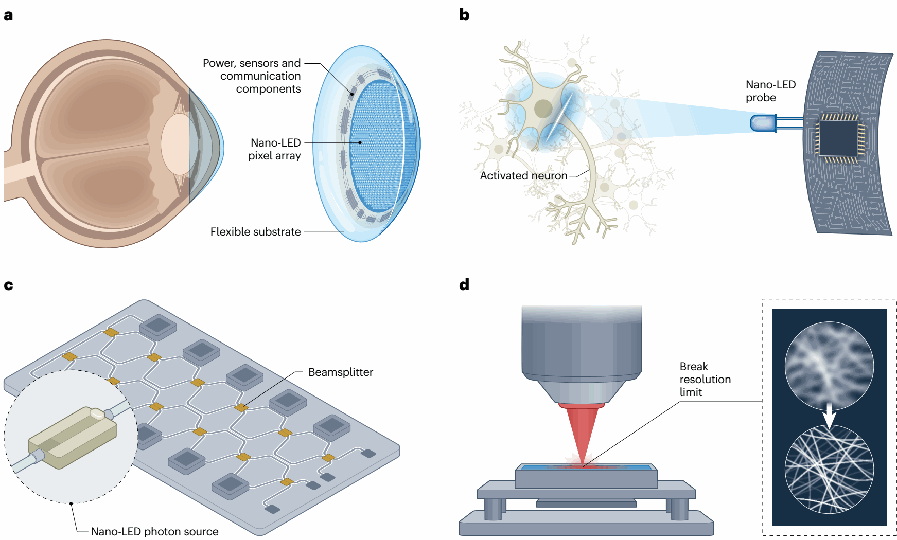
Nano-LEDs for cutting-edging applications
The paper further outlines the application potential of nano-LEDs beyond displays. In the field of biophotonics, ultracompact arrays are expected to be used for contact lens microdisplays and finer optogenetic neural modulation, but issues such as biocompatibility, thermal management and long-term stability still need to be addressed; in the field of optical interconnects, localized light emission and fast modulation capabilities provide research ideas for short-distance information transmission among chips, circuits and photonic modules; in the field of super-resolution microscopy imaging, the proposed nano-illumination imaging scheme uses independently addressable nano-light-source arrays to provide localized illumination near the sample, and is expected to improve imaging resolution by reducing light source size and spacing.
Starting from the relationships among material surface chemistry, nanofabrication and device working mechanisms, this review systematically elaborates the material foundations, key bottlenecks and development directions for achieving high-density integration of solution-processed nano-LEDs, providing a reference for research on ultrahigh-resolution displays, miniature biophotonic devices and on-chip photonic systems.
Article link: https://doi.org/10.1038/s41566-026-02010-1
Editor: Liu Tingting


 Beihang NewsBeihang holds 2026 Alumni Homecoming and Innovation Development ConferenceMore
 Beihang NewsBeihang Aeromodelling Team secures four championships, two runners-up and one third place at CUADC 2026More
 Beihang NewsICBE 2026 convenes in BeijingMore
 Beihang NewsKenya Space Agency Director General and Beihang alumnus Hillary Kipkosgey returns to campusMore
 Beihang NewsBeihang hosts 64th Faculty and Student Sports MeetMore
 Beihang NewsVice governor of Shanxi Province visits Beihang UniversityMore